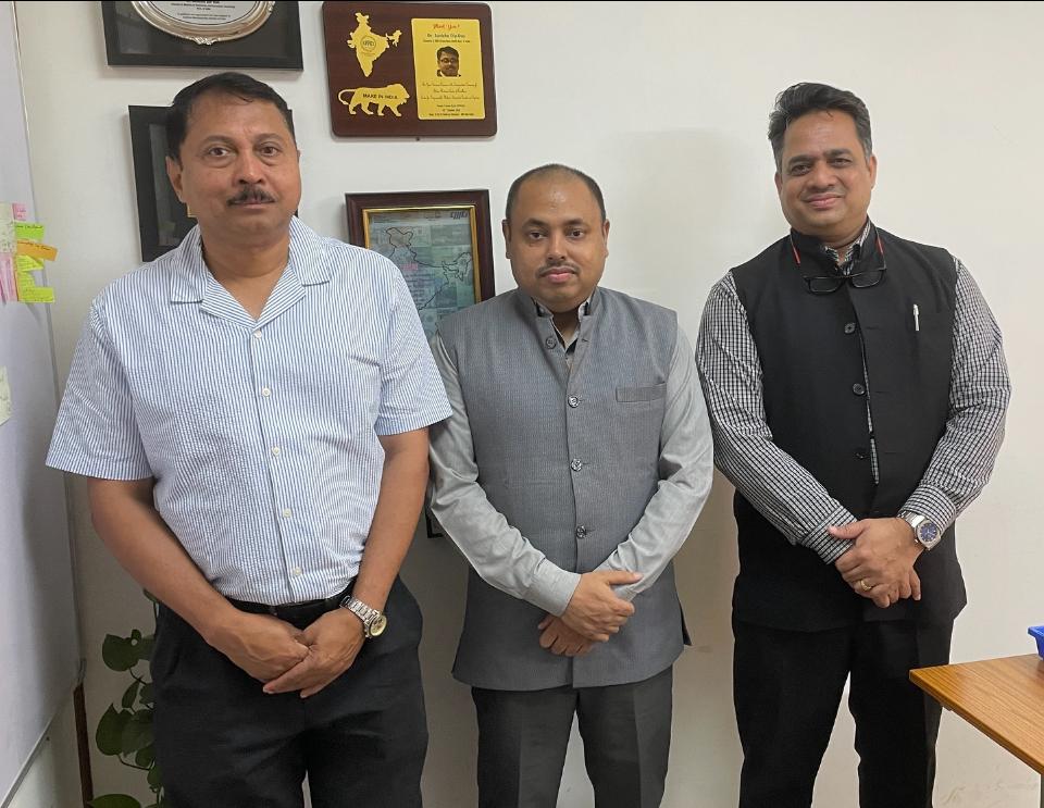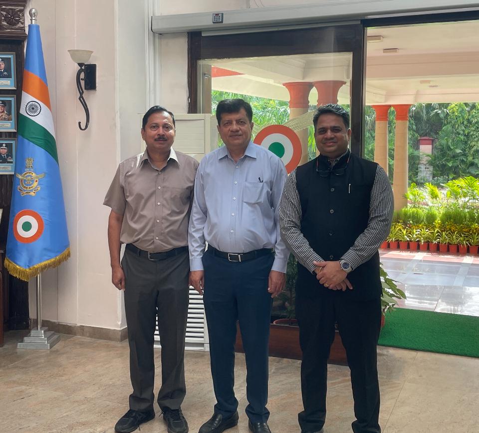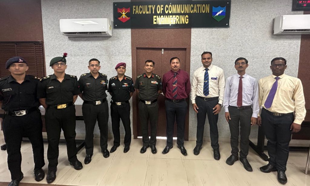
3D GRAPHY KNOWLEDGE FORUM – presentation on 3D printing in electronics and semiconductors was presented to Brigadier Rajesh Verma, Head of Electronics at the Military College of Telecommunication Engineering in Mhow, as a demonstration of the potential of 3D printing in advancing military technology.
The meeting was initiated by Cmde. Niranjan Khardenavis ( Retd.) Ex- CTO, Indian Navy, Associate Director, Defence & Marine, 3D GRAPHY LLP. Members who joined included Dr. Sankha Dip Das, Scientist “E” , Ministry of Electronics & Information Technology, Govt. of India, Dr. Shany Joseph, Scientist “E”. CMET Pune, Dr. Shibu John, CEO & Founder, 3D GRAPHY LLP, Founder & Secretary, 3DPERA, Dr. Winstone Deaver, Research Engineer, 3D GRAPHY LLP, Mr. George K John, Business Associate, Engineering & Marine, 3D GRAPHY LLP, Ms. Tejal Modi, Head PR & Communications, 3D GRAPHY LLP & Editor, 3D Graphy News.
Presentation was made by Dr. Winstone Deaver, PhD Additive Manufacturing, Research Engineering, 3D Graphy, Dr. Shany Joseph, Scientist “E”, CMET Pune joined by Dr. Sankha Dip Das, Scientist ” E” , Ministry of Electronics & Information Technology, Govt. of India.
Title Slide
- Title: 3D Printing in Electronics and Semiconductors
- Subtitle: Revolutionizing Military Technology
- Presented by: Dr. Winstone Deaver, PhD Additive Manufacturing, Research Engineer, 3D GRAPHY LLP, Dr. Shany Joseph, Scientist ” E”, CMET Pune.
- For: Brigadier Rajesh Verma, Head of Electronics, Military College of Telecommunication Engineering, Mhow
- Date: 21th August 2024.
Introduction
- Overview of 3D Printing in Electronics and Semiconductors
- Brief history and evolution of 3D printing in electronics.
- Importance of 3D printing for the military and defense sectors.
Applications of 3D Printing in Electronics
- Printed Circuit Boards (PCBs)
- How 3D printing can create complex, multi-layer PCBs.
- Advantages in rapid prototyping and small-scale production.
- Antennas and Sensors
- 3D printing of customizable and lightweight antennas.
- Integrating sensors directly into 3D-printed devices for field applications.
- Flexible Electronics
- Wearable technologies and conformal electronics for soldiers.
- Examples of flexible displays and sensors used in military gear.
3D Printing in Semiconductor Manufacturing
- Microelectronics and Semiconductor Devices
- 3D-printed transistors and microchips: current capabilities and future possibilities.
- Potential for creating custom semiconductor devices for specific military applications.
- Integration with AI and IoT
- How 3D printing supports AI-driven electronics and IoT devices in the field.
- Real-time data collection and processing through 3D-printed semiconductor devices.
Advantages of 3D Printing in Military Electronics
- Cost Efficiency
- Reduction in costs associated with traditional manufacturing.
- Economies of scale for small-batch production.
- Rapid Prototyping
- Quick turnaround from design to deployment.
- Adaptation to battlefield requirements with on-site 3D printing.
- Customization and Miniaturization
- Tailoring electronics to specific missions or individual soldier needs.
- Miniaturizing components to reduce weight and increase portability.
Challenges and Future Directions
- Technical Challenges
- Material limitations and reliability concerns.
- Integration with existing manufacturing processes.
- Future Trends
- Evolution towards fully integrated 3D-printed electronic systems.
- Collaboration between military, academia, and industry to advance research.
Conclusion
- Summary of Key Points
- Reiteration of the benefits of 3D printing in electronics and semiconductors for military applications.
- Call to Action
- Encouraging the adoption of 3D printing technologies at the Military College of Telecommunication Engineering.
- Proposal for a pilot project or further research collaboration.
- Setting up a 3D GRAPHY HUB in the Institute.
Q&A
- Open Floor for Questions and Discussion
This outline can be tailored with specific data, visuals, and examples relevant to Brigadier Rajesh Verma’s interests and the strategic goals of the Military College of Telecommunication Engineering. A proposed a visit to the CMET Pune will be initiated soon for understanding the application and connecting dots for addressing different problem statements using 3D technology.
Dr. Shibu John, CEO & Founder, 3D Graphy LLP, Organising Committee Member, 3D GEM 2024 also invited all the respondents in the meeting to participate in the 3D GEM 2024 event held in IIT Delhi on 9th & 10th November jointly organised by IIT Delhi & 3D Graphy.